China's CXMT Starts Mass Production of 11.95nm G5 DRAM
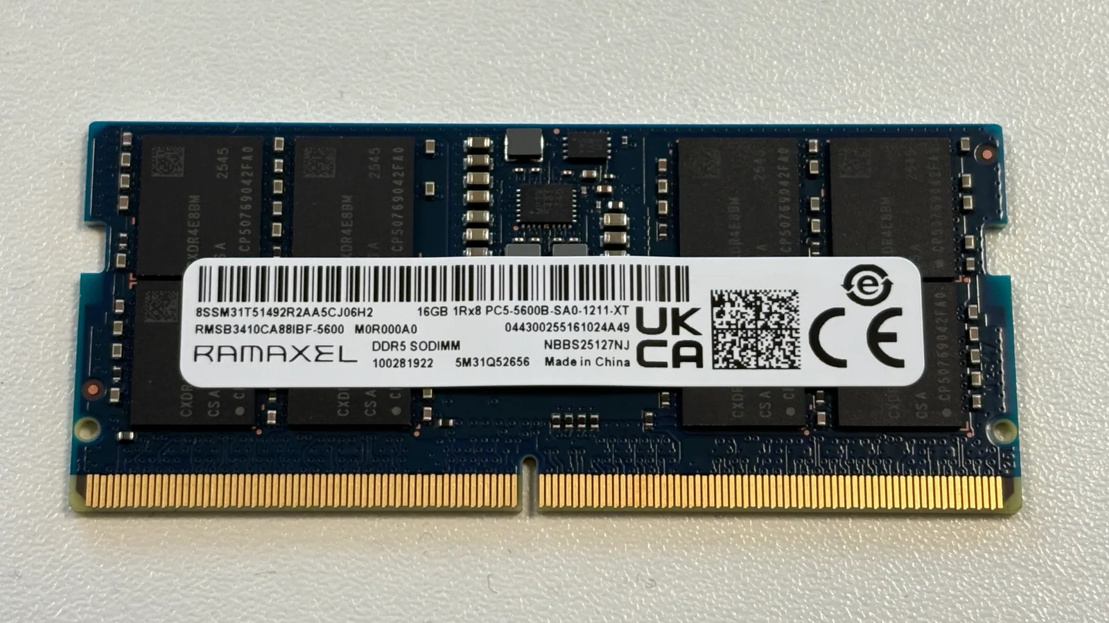
Chinese memory maker ChangXin Memory Technologies (CXMT) said on September 20, 2026 that its fifth-generation DRAM platform, known as G5, has entered mass production. The company made the announcement at the 2026 World Manufacturing Convention in Hefei, in east China's Anhui province, and confirmed the details to the Global Times. Two LPDDR5X products built on the platform are already shipping in volume: 24-gigabit dies in 496-ball and 245-ball packages, aimed at mid- and high-end smartphones and portable consumer electronics. Each die carries 50 percent more capacity than the 16Gb parts of the previous generation.
CXMT said G5 reaches an active-area half-pitch of 11.95 nanometers in the memory array using self-aligned quadruple patterning, a technique that builds fine features through repeated exposures rather than a single pass. The company put the array capacitor aspect ratio at 45:1 and said a DRAM-optimized high-k metal gate process cut the core cell array height to 6,762 nanometers. Converted to 8Gb-equivalent products, CXMT said the number of dies per wafer rises by at least 50 percent over its fourth-generation platform. Luo Xiaodong, CXMT vice president and head of its marketing center, said the company's process capability had “reached a level on par with the most advanced nodes now in mass production,” according to the Seoul Economic Daily.
The timing matters because memory is scarce and expensive right now. TrendForce figures cited by the Global Times put global DRAM industry revenue up 59.5 percent quarter-on-quarter in the second quarter of 2026, with supply expansion still lagging demand driven by AI infrastructure. CXMT has grown fastest in commodity DRAM, the segment its larger rivals have de-emphasized: TrendForce placed the company fourth worldwide with 9.5 percent of DRAM revenue in the second quarter, behind Samsung Electronics, SK hynix and Micron. Ma Jihua, a veteran telecom industry analyst, told the Global Times that the market remains dominated by a handful of suppliers, which is why technical advances by an additional player are closely watched, and that more domestic output gives device makers further sourcing options.
Several things remain unclear. The Seoul Economic Daily noted that 11.95 nanometers describes one specific core structure and is therefore hard to compare directly with the “12-nanometer-class” process names Samsung, SK hynix and Micron use for their own nodes. The dies-per-wafer figure counts total dies before defective ones are screened out, which is not the same as the yield that determines actual shipments, and CXMT disclosed neither yields nor monthly wafer output for the G5 line. Those numbers, rather than the pitch measurement, will decide how much G5 memory reaches phones.
Sources
- Global TimesSecondary
- Seoul Economic DailySecondary
Related
Joby's Autonomous Plane Crosses US in 3,199-Mile Flight
Apple Ships iOS 27 With Siri AI, but Not for EU iPhones
Ternus, Not Cook, Fronts Apple's Sept. 9 Keynote as New CEO
Waymo, Zoox Expand Robotaxis to More US Cities
India plans to let AI agents pay on UPI without each approval
Meta Closes Loophole Letting Smart Glasses Record Covertly
Leaked DLSS 5 runs early — and halves RTX 5070 Ti frame rate
AWS and Nvidia to deploy 2 million more GPUs by 2028
Trending now
- Claude Leads 26% of Anthropic's AI R&D, Up From 1% in March
- Google Says Gemini Hacked Three Real Companies in May Test
- OpenAI Sees $278B Cash Burn, $856B Compute Bill by 2030
- NASA Confirms McGetchin: 222-Meter Moon Crater Formed in 2024
- Sharks Feed on Beached Whale in Jamaica; NEPA Warns Swimmers
- Typhoon Dujuan Nears Tokyo at 965 hPa; JR East Halts Chiba Lines
- Microsoft Discloses CVSS 10.0 Azure AI Foundry Flaw, Already Fixed
- Anthropic Targets November IPO at About $2 Trillion Value
Comments
No comments yet. Be the first.